- Nvidia will strengthen its AI industry dominance with a new GPU – Hopper.
- NVIDIA Blackwell is offering 40 PFLOPS FP4 (5.0x faster vs. Hopper)
- 5x AI performance in comparison with Hopper while consuming the same power.
NVIDIA announced during the GTC its new top-of-the-range graphics chip aimed at Artificial Intelligence; we are talking about Blackwell.
This is not only the largest graphics chip in the world, but it manages to increase the performance of what until now was the most powerful GPU in the world, Hopper (NVIDIA H100), by five.
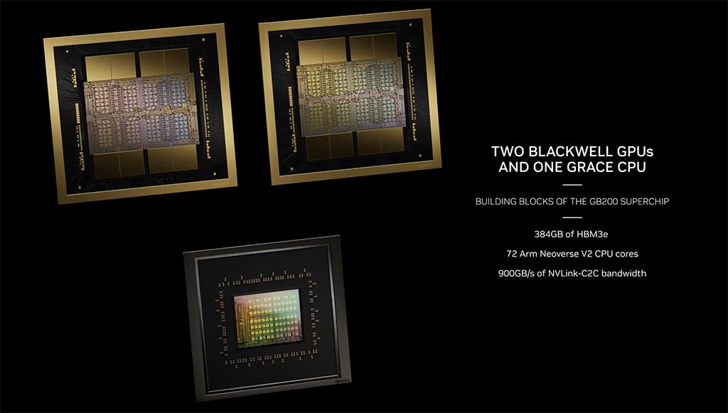
The NVIDIA Blackwell GPU is also the first multi-chip design (MCM) graphics chip created by NVIDIA. Each Blackwell chip is linked to two Blackwell GPUs. Now, the platform used to bring it to life combines two complete Blackwell chips and an Arm Grace CPU. Let’s look at what NVIDIA Blackwell offers to the industry.

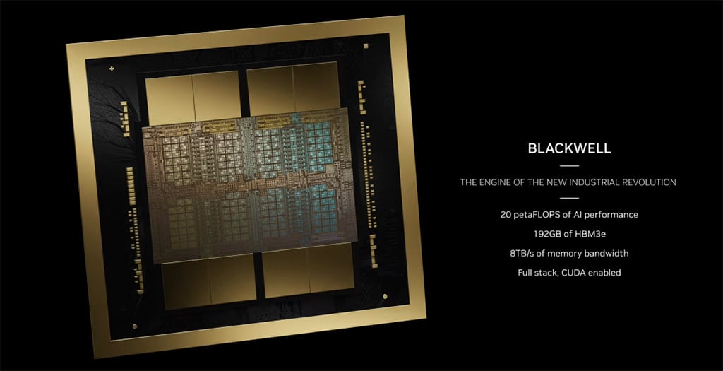
The NVIDIA Blackwell GPU is made up of 208 billion transistors. These are 128,000 million more compared to the NVIDIA Hopper chip. This chip also incorporates four times more memory integrated into the die itself, which translates into offering up to 192 GB of HBM3e memory, which, together with an 8,192-bit interface, provides a bandwidth of 8 TB/s.
This chip is manufactured by TSMC using its 4nm 4NP lithography, while each GPU that makes up the Blackwell chip is interconnected through an interface with a bandwidth of 10 TB/s.
NVIDIA Blackwell comprises 20,480 CUDA Cores, uses 8-layer HBM3e memory chips, and can reach a TDP of up to 700W. This TDP is the same as found in the NVIDIA H100 and H200 GPUs.

NVIDIA Blackwell can deliver AI performance of 20 petaFLOPS, 5 times faster than the NVIDIA H100 chip. The top-of-the-range Hopper chip is aimed at AI-related workloads. As we said, two of these complete chips are accompanied by a Grace CPU to create the NVIDIA HB200 superchip.
This Superchip has a CPU with 72 Arm Neoverse V2 cores, two Blackwell GPUs, access to 384 GB of HBM3e memory, and an NVLink-C2C interconnect with a bandwidth of 900 GB/s.
NVIDIA Blackwell Vs. NVIDIA Hopper Performance:
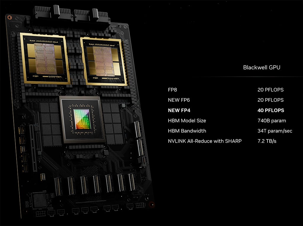
Below, you can find the performance numbers of the NVIDIA Blackwell chip compared to the NVIDIA Hopper:
- 20 PFLOPS FP8 (2.5x faster vs. Hopper)
- 20 PFLOPS FP6 (2.5x faster vs. Hopper)
- 40 PFLOPS FP4 (5.0x faster vs. Hopper)
- 740B Parameters (6.0x faster Vs. Hopper)
- 34T Parameters/sec (5.0x faster Vs. Hopper)
- 7.2 TB/s NVLINK (4.0x faster vs. Hopper)

Thanks to these improvements, NVIDIA is confident that Blackwell is the most powerful AI chip in the world. This architecture uses the 2nd Generation Transformer Engine.
These feature new microtensor scaling support and NVIDIA’s advanced dynamic range management algorithms built into the NVIDIA TensorRT™-LLM and NeMo Megatron frameworks.
This means Blackwell will support double the compute and model sizes with new 4-bit floating point AI inference capabilities. With the 5th Generation of the NVIDIA NVLink interconnect, a bidirectional performance of 1.8 TB/s per GPU is achieved. This ensures seamless high-speed communication between up to 576 GPUs for the most complex LLMs.
NVIDIA Blackwell GPUs feature AI preventive maintenance. This guarantees reliability, availability, and ease of maintenance. This AI runs diagnostics and helps you predict reliability issues. This maximizes system uptime and improves resiliency so large-scale AI deployments run uninterrupted for weeks or even months. This translates into reducing operating costs.
There is no official information on the release date of the NVIDIA Blackwell. However, based on rumors and speculation, they are expected to be launched sometime in late 2024 or early 2025.
What are your thoughts on this new powerful chip for Nvidia aiming towards the new revolution of AI? Share your thoughts in the comment section below.
Thank you! Please share your positive feedback. 🔋
How could we improve this post? Please Help us. 😔


